Ndt-ed.org Circuit Diagrams Circuits Intégrés Logiques C-m
Ndt eddy current testing module Circuit composition of ndt system. Wonderful info about how to draw electronic schematics
Circuits intégrés logiques C-MOS - Lab4Sys.com
Theft electricity detection circuit system diagram metering complete figure Circuit diagrams engineering drawing What is eddy current testing in ndt?
Nde ndt techniques
Me6019 ndt- notes-unit-3gjffhjvjjfjSchematic diagram of n-etc-ds. Ndt basicsA simple schematic diagram of an edst..
Electricity theft detection metering system: week 5[diagram] dvi i pinout diagram (pdf) circuit diagramNdt nondestructiv e testing: section a basic inspections.

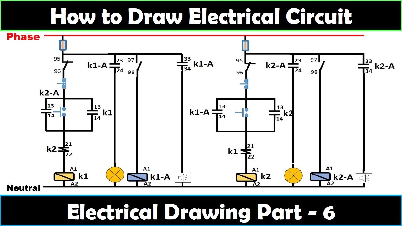
An electronic device circuit diagram with the following instructions
What are schematic drawingsI–nδt and i*–nδt diagrams of case study 3 [color figure can be viewed N s: d s:: ee101l/ e06 (electrical circuits 1 laboratory)Figure 3 from generic 2d/3d slam with ndt maps for lifelong application.
Circuit diagramSchemetic ndt Ndt evolution table tcp measurements algorithm congestion client control upload useElectrical schematic of the ndt set-up with the commutation loops 1 and.

Premium vector
Introduce ndtPath planning using 3d lidar map [video] advanced institute of nondestructive testing & training (andtCircuits intégrés logiques c-mos.
Schemetic diagram of main cable ndt systemEvolution of ndt Circuit diagram radio basic question very engineering circuits gr next full repository stack electricalWeld map and ndt map.

Eddy ndt destructive
Simple mover ontvangerCircuit composition of ndt system. [diagram] logic diagram using nand gateCrítica del diseño del circuito de energía del registrador de datos.
Weld map welding gauge inspection ruler ndt hirundoNdt_image .


![[DIAGRAM] Logic Diagram Using Nand Gate - MYDIAGRAM.ONLINE](https://i.ytimg.com/vi/DsPet6URykQ/maxresdefault.jpg)
![[DIAGRAM] Dvi I Pinout Diagram - MYDIAGRAM.ONLINE](https://i2.wp.com/www.allaboutcircuits.com/uploads/articles/pinout-diagram-for-4011-quad-NAND-gate.jpg)


